Populärvetenskaplig presentation
It is not always easy to explain what a solar cell is, how it works and how it is made. Here we have made a popular science presentation to explain more.
The history of solar cells
The history of solar cells dates back to the 19th century, when the mechanism by which light can create a voltage was discovered. Since then, a spectrum of materials and technologies for extracting energy from sunlight has been developed and solar cells can be used in many different types of systems. More recently, solar energy has received increasing attention as it offers a renewable way to generate electricity.
The importance of semiconductors
All solar cells have in common that they need a layer that absorbs the light, where a semiconductor is often used. Semiconductors are defined by that their electrons just fill up a valence band where they do not conduct a current, but that the electrons can be excited to a conduction band where they can move freely. In a solar cell, the photons in the sunlight will provide energy for the electrons to be excited. When an electron has been excited it needs to be separated from the hole it left behind, and therefore the absorber layer is made of two materials – one semiconductor that has been doped with a shortage of electrons, p-doped, and one semiconductor that has been doped with a surplus of electrons, n-doped. When these are united a so called pn-junction is formed between the semiconductors where the difference in the amount of electrons is evened out which creates an electrical field. The energy levels for the valence band (Ev) and the conduction band (Ec) will now look as in the picture. The distance between them is intrinsic for the material and is called the bandgap (Eg).

Banddiagram för en solcell.
When a photon excites an electron near this electrical field, the electron will be transferred by the field and thereby separated from its hole which gives rise to a potential difference between the sides. Both the electron and the hole can here be seen as particles contributing to the current and they can both be called charge carriers. In reality, a hole current consists of different electrons continuously filling the next hole and leaving a new hole behind, but it is easier in practice to deal with holes as their own particles. On each side of the absorber layer there will be contacts that conduct the charge carriers to and from the absorbing material, and if these are connected in a circuit they will conduct an electrical current. This way a direct current has been formed from the excited electrons. For the absorber to be reached by the light the front contact must be transparent to visible light, which is therefore called the window layer.
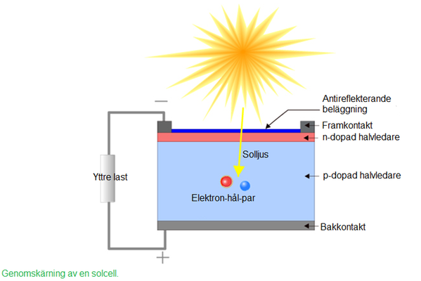
Tvärsnitt av en solcell. Bilden från pveducation.org.
The picture above is retreived from pveducation.org.
To make the solar cell efficiency as high as possible you have to minimize all its losses, and to investigate its performance the solar cell can be characterized in different ways. An example of this is IV-measurements, where the current through the solar cell is related to the voltage over it. This curve provides some important parameters that describe the solar cell. One of these is the short circuit current (Isc) which represents the current when the positive and negative contacts are directly connected and the solar cell is short-circuited. On the other hand, there is an open circuit voltage (Voc) which is the voltage when the circuit is open and no current is present. To calculate the maximum power (Pmp) from the solar cell a parameter called the Fill Factor (FF) is used. This measures how close to square the IV-curve is. The parameters are connected as Pmp=Voc*Isc*FF, and the total efficiency can be calculated as the ratio between Pmp and the total power that has been added to the solar cell.
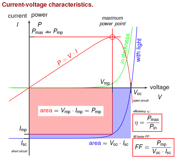
Egenskaper ström-spänning.
Even if you have a solar cell with very high performance there is a maximum theoretical efficiency limit of 33 % that cannot be exceeded. The main reason for this is because the solar spectrum is rather wide and the solar cell is most effective for photons with the same or somewhat higher energy than the material’s bandgap. Generally, the losses in the solar cell can be divided into four types: generation losses, thermalization losses, recombination losses and resistive losses. Generation losses describe the losses in generating electron-hole pairs from the incident light. This is for example due to that a part of the irradiating light is reflected at the surface or absorbed already in the window layer, which is called parasitic absorption. There is also a cut-off where the incoming photons has lower energy than the bandgap and therefore cannot be absorbed to generate pairs. Thermalization losses occur because photons with higher energy than the band gap can only excite one electron, and the surplus energy is released as thermal energy. Recombination describes when electrons are de-excited to a hole and release its energy, and it therefore no longer contributes to the electricity generation. This type of loss is common for example in interfaces and at defects in the material that could give middle-steps on the way down to the hole. Resistive losses consist of series resistance and shunt conductance. Series resistance is the resistance for the current to pass through the material and contacts and shunt conductance is when faults in the material lead to shortcuts for the current so it doesn’t pass through the solar cell.
In thin film solar cells materials are used that are very efficient in absorbing light. This is because they have a direct bandgap, which means that the electrons can be excited just with light absorption. Silicon, for example, has an indirect bandgap where the photon cas to be caught simultaneously as the electron interact with the crystal to change its state, and therefore the absorption is not as probable. Therefore, the layers in the thin film solar cell can be made much thinner than the conventional solar cell. However, since they are so thin they cannot hold up their own weight but must be deposited on a substrate, for example glass, metal or plastics, but it could also be an advantage since they can be made flexible.
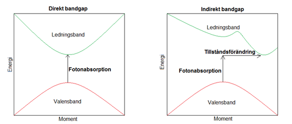
Direkta och indirekta bandgap i halvledare.
At Uppsala University there is research on the materials CIGS, which is an abbreviation for Cu(In,Ga)Se2, and CZTS, which means Cu2ZnSn(S,Se)4, that are both used for thin film solar cells. For manufacturing solar cells you first have to deposit a back contact of molybdenum (Mo), which works as the positive contact if you compare solar cells to a battery. On the back contact the absorber layer of CIGS is deposited for the sun absorption. Between this and the front contact there is a buffer layer to passivate the surfaces and improve the optical and electronic properties between the absorber and the front contact. The buffer layer usually consists of cadmium sulfide (CdS). To finish the solar cell a front contact (with negative polarity) of intrinsic (nondoped) and finally aluminum doped zinc oxide (i-ZnO and ZnO:Al) is deposited. For CZTS-solar cells, the absorber layer will instead consist of the CZTS-material and it might be advantageous with other choices of materials as buffer layer.
To make the solar cells as efficient as possible the material needs to be very pure and cannot be polluted with other compounds that may reduce the light absorption or the electricity production. Therefore, the development of the solar cells is conducted in a clean room where the number of particles in the air is minimized. In the clean room many machines are used to manufacture and characterize solar cells. For depositing the different layers of the solar cells there are different methods. With co-evaporation, the elements to be deposited are heated up to evaporate in a vacuum chamber and are then condensed on the substrate in the chamber. With sputtering, a target with the elements is instead bombarded with non-reactive ions in a gas which makes atoms eject from the target and deposit on the substrate. There is also equipment for characterizing the materials that are created, for example different kinds of spectroscopy and microscopes.
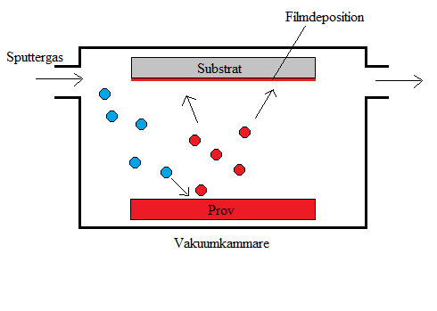
Tekniker för samförångning (a) och sputtring (b) som används vid tillverkning av solceller.
The overall goal of the research is to improve the efficiency of the thin film solar cells. This is achieved by developing the material in different ways, for example combining different materials to make the cell and to research the processes that affect the material properties. With a higher efficiency, more of the sunlight can be transformed into electricity and be useful in our energy system.