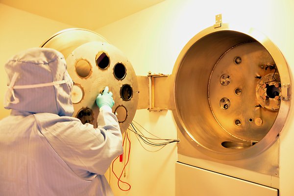
High-current implanter
For ion implantations as well as ion beam analysis methods using keV ions, the Tandem laboratory features a Danfysik 1090 accelerator platform. The machine is equipped with a highly versatile ion source that allows us to produce ion beams from almost all elements of the periodic table for a wide range of applications. The ions are accelerated with up to 350 kV and steered into one of three beamlines for different applications.
The first beamline is dedicated to implantations and irradiations. Beam currents of up to a few mA enable high-dose implantations even on large targets.
The second beamline consists of our unique time-of-flight medium-energy ion scattering system used for high-resolution depth profiling and crystallography of thin films.
Finally, the third beamline extends to a multipurpose scattering chamber. Most prominently, the set-up allows to depth-profile ¹¹B and ¹⁸O using nuclear reactions.
Implantations of various ion species for a large number of different applications are regularly requested both from industry and academic researchers. The wide range of available ion species allows us to address different requests from typical semiconductor dopants (B, Al, P, As, and others) over different metals (for example Fe, W) to light and heavy noble gases. We can vary irradiation flux and dose and, due to the high achievable beam current, can even perform implantations at very high doses.
The target chamber is accessed via a clean room environment to ensure ultra-clean surfaces during sample preparation and mounting
Features
- Wide range of ion species.
- Deceleration unit in the beamline to allow for ion energies down to 2 keV.
- Beam scanning and focussing for homogeneous exposure over large areas.
- Maximum target size: ∅ 6''. Standard sample holder available for 2'', 4'' and 6'' samples.
- Water cooling of the sample holder.
- Hot implantations at temperatures up to 650°C possible.
- Adjustable incident angle between the ion beam and the target surface.
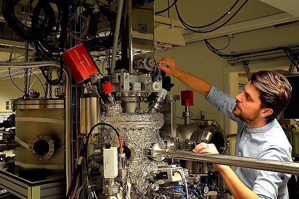
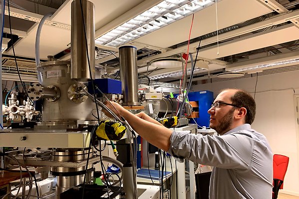
The time-of-flight medium-energy ion scattering (ToF-MEIS) system is our own design and combines pulsed keV ion beams with advanced detection systems. This unique set-up is developed for analysing the chemical composition and crystallographic structure of thin films with very high depth resolution and in a non-destructive manner. Another focus lies on fundamental research on ion-solid interactions.
In the beamline, the keV ion beam coming from the implanter platform is divided into short pulses with a length of about 1 nanosecond. A drift tube buncher can additionally be used to decrease pulse widths to about 0.3 ns. This division in time allows scientists to measure energy with very high resolution, which is beneficial for fundamental studies as well as for achieving high depth resolution.
The scattering chamber features two detectors. The first one is movable and can be placed at any scattering angle for measurements in backscattering, forward scattering and transmission geometry. Its large area allows for short measurement times as well as angle-resolved measurements and real-space crystallographic images. The second detector is mounted at a fixed position further away from the sample position resulting in enhanced time resolution which translates to sub-nm depth resolution. The detector type we are using is not only sensitive to ions but also capable of detecting neutral atoms, electrons, and photons.
The ToF-MEIS system is complemented by a sample preparation chamber allowing for growth of thin films and preparation of surfaces for in-situ studies of surface science effects.
A versatile time-of-flight medium-energy ion scattering setup using multiple delay-line detectors
Part of Nuclear Instruments and Methods in Physics Research Section B, p. 16-20, 2020
Part of Review of Scientific Instruments, p. 95107, 2012
Features ToF-MEIS system
- Non-destructive measurement technique due to use of a pulsed ion beam.
- Sample mounted on 6-axes goniometer allowing for 3 translational and 3 rotational movements.
- Sample holder for transmission experiments on self-supporting foils available.
- In-situ annealing at up to 600°C.
- Possibility to vary the potential of the sample holder between -500 V and 500 V, thereby allowing for the detection of low-energy secondary ions and electrons.
- Two microchannel plate (MCP) detectors coupled with two delay lines each to record particle energy as well as position.
- First detector: rotatable around the scattering point with a large solid angle of 0.13 sr.
- Second detector: fixed at a backscattering angle of 135° at a distance of 1050 mm for enhanced energy resolution.
- Possibility to measure the exit charge state during ion transmission experiments.
- Charge deflection electrode in front of the second detector to separate neutrals from ions.
- Chamber base pressure: <3 x 10⁻⁸ mbar.
Features sample preparation chamber
- 2 electron-beam evaporators, both capable of accommodating crucibles and rods, and operable at the same time for (co-)deposition of thin films.
- 1 additional magnetron sputtering unit operable in DC or RF mode.
- Gas inlet making reactive deposition processes possible.
- keV sputter gun including Wien Filter.
- Annealing of samples at temperatures up to 1200°C using an electron-beam heater.
- Retractable button heater allowing for annealing at up to 500°C of even self-supporting targets.
- Residual gas analysis during operation.
This beamline is dedicated to sub-MeV ion beam analysis. Multiple detectors allow for near-surface materials characterisation with high resolution. A unique feature of this set-up is the usage of two nuclear resonances of keV protons: at 151 keV with ¹⁸O and at 163 keV with ¹¹B. By detecting the resulting alpha particles, these isotopes can be quantified depth-resolved permitting isotope-selective studies of materials diffusion. This capability has also been used to quantify boron in transition-metal borides, which are technologically relevant for coatings or as friction materials.
Other techniques available are high-solution backscattering spectrometry, also in combination with channelling, and low-energy PIXE for detection of elements as light as carbon.
Part of Nuclear Instruments and Methods in Physics Research Section B, p. 104-110, 2020
Systematic compositional analysis of sputter-deposited boron-containing thin films
Part of Journal of Vacuum Science & Technology. A. Vacuum, Surfaces, and Films, 2021
Features
- Large-area (1200 mm2) passivated implanted planar silicon detector (PIPS) with absorbers to detect alpha particles from nuclear reactions.
- Surface barrier detector (SBD) with cooled preamplifier electronics for high-resolution backscattering spectrometry. For protons and deuterons typical resolutions of 3 keV (FWHM) can be achieved.
- Ultra-fast silicon drift detector (SDD) with very thin Be-window layer to detect characteristic X-rays from elements with Z ≥ 6.
- Sample holder attached to remotely controlled 3-axes goniometer.
- Beam currents up to µA achievable.
- N2-trap to improve the chamber base pressure to <10-7 mbar.