Research Methods
Here you can find an overview of the materials synthesis and analysis methods we use in our research.
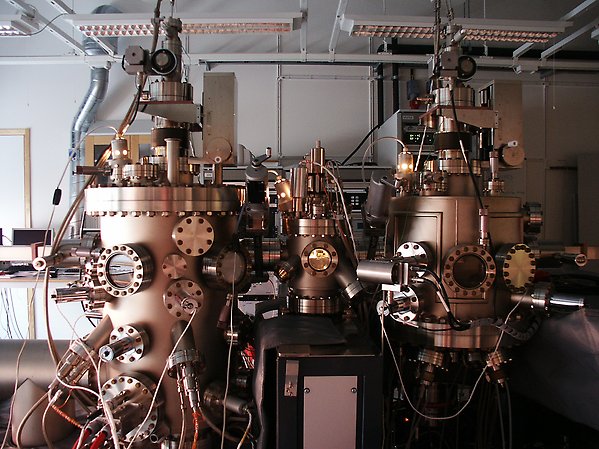
The synthesis of new materials is central to our research. Single crystalline as well as amorphous materials can be grown by the use of magnetron sputtering and/or Molecular Beam Epitaxy (MBE). Using these methods we can create phases that do not exist naturally.
The use of magnetron sputtering or molecular beam epitaxy makes it possible to fabricate thin films with physical properties which differ significantly from those of bulk materials. Layers of different materials can be deposited with thickness control on the sub-Ångström level through computer controlled opening of shutters in front of the growth sources. By simultaneous co-deposition from several sources one can produce alloys where the composition is largely determined by the electrical power on each source.
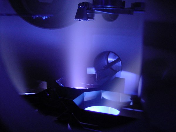
Compounds such as oxides can also be deposited, either using a source of the desired composition or by reactive sputtering, where a reactive gas (oxygen in the case of oxide deposition) is used in the sputtering chamber. Using multiple confocal sources placed at an angle with the substrate surface, one can produce thin films with a compositional gradient, in a process known as combinatorial materials synthesis. This allows an efficient mapping of properties for a large range of compositions in a single sample. 3 inch wafers can be coated in this way, with up to four material sources, allowing for complex quaternary alloys to be studied.
Sputtering is an extremely versatile process and a large range of process parameters such as sputter gas pressure and composition, target power, and sample bias voltage can be adjusted to tune the film properties. One necessary prerequisite for film quality is an extremely pure environment to reduce the level of contamination to an acceptable level in the samples. Therefore, deposition takes place in ultra-high vacuum chambers with background pressures below 10-9 mbar.
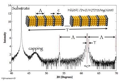
X-ray diffraction is the standard method for determination of crystal structures. Rutherford backscattering allows us to measure the chemical composition of our films.
Information about crystal structure (or lack thereof), layering and interfaces can be obtained through X-ray scattering experiments in a range of different scattering geometries. Careful analysis of such measurements (using computer codes developed within the group) are the primary source of information about the structural properties of our samples.
In the specialized equipment in the Materials Physics group, samples can be exposed to controlled hydrogen pressure during measurements. Crystallographic changes (rearrangements, phase transitions) can be followed in-situ at different selected pressures and temperatures in the interval 10-800 K during hydrogen uptake, even for nano-sized layers (> 50 Å).
Rutherford backscattering (RBS) and nuclear reaction analysis (NRA) are used for determining the chemical composition of thin films, multilayers and superlattices. These techniques are based on swift ions impinging on the material, resulting in scattering, electronic excitations and if the energy is high enough, nuclear reactions. A combined NRA / RBS system is located at the Tandem accelerator in the Ångström Laboratory. This setup has unique capabilities: it is ultra-high vacuum based and it combines total integration of the incoming particles and the samples can be cooled during ion bombardment (which is extremely important for analysis of light elements such as hydrogen, where there is a risk for ion beam induced desorption of the material). The NRA facility is the only one of its kind in Sweden.
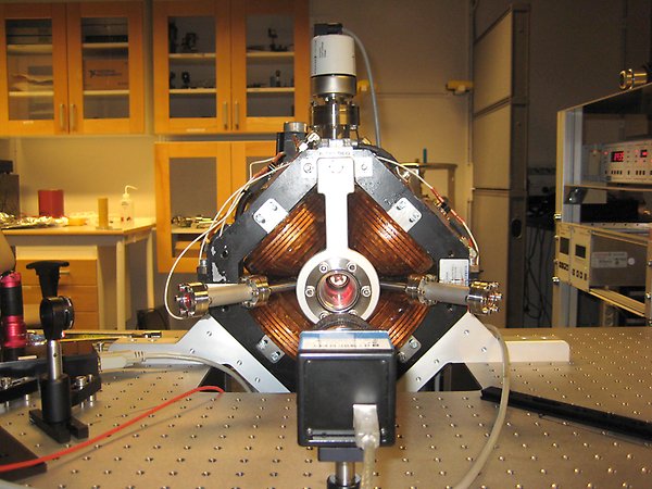
The magneto-optical Kerr effect (MOKE) provides a convenient way to obtain the changes in magnetic moment at different fields and temperatures. We have several experimental setups using this effect.
When linearly polarised light reflects from a magnetic film, its polarisation becomes elliptic and the principal axis is rotated. The amount of rotation and ellipticity is proportional to a component of the magnetisation of the film. Which component is measured depends on the optical configuration used. Polar MOKE measures the out-of-plane component, whereas transverse and longitudinal (with an angle of incidence not perpendicular to the sample surface) measures in-plane components to a depth of some 20 nm in metals.
Hysteresis, M(H), loops, with shapes strongly dependent on e.g. anisotropy or interlayer coupling, are conveniently measured at room temperature or under other conditions, depending on which setup is used. For investigations of e.g. magnetic phase transitions, a set-up with extremely low background fields (less than 10 μT) is used. Here we can measure both AC susceptibility, dM/dH, and low-field M(H) loops at different temperatures below 300 K. The sensitivity allows studies of even just a few monolayers of magnetic material.
At the other extreme, some samples need higher fields to reach saturation. The Vector MOKE setup combines all the three configuration modes with different wavelengths (spectroscopic MOKE; all elements respond differently to the incident light), a relatively high field, and a temperature range 4 – 500 K. Simultaneous measurement of the first harmonic (ellipticity) and second harmonic (rotation) of the modulated reflected light allows determination of the scaling of magnetisation with field in the vicinity of the ordering temperature as well as separation of the contribution from different elements in multilayered structures.
It is possible to see magnetic domains! It is even possible to distinguish between different directions of the magnetisation.
Compared to e.g. magnetic force microscopy the Kerr microscopy method has the advantage of directly monitoring the in-plane and out-of-plane magnetization components. Furthermore, Kerr microscopy can be used in a wide range, visualizing domains in the range of 0.0003 mm to a few mm. The resolution is limited, by the wavelength of the visible light, to roughly 0.0003 mm.
Depending on the relative orientation of the incident light, the applied magnetic field, and the domains, patterns of black, white and greys are obtained. A large black and white contrast is obtained from areas with opposite magnetization directions.
The microscope is operated using polarized light, with an electromagnet around the sample position and adjustable illumination to optimize the contrast. It can also be equipped with cooling stages for studies of temperature dependence of domain formation and dynamics.
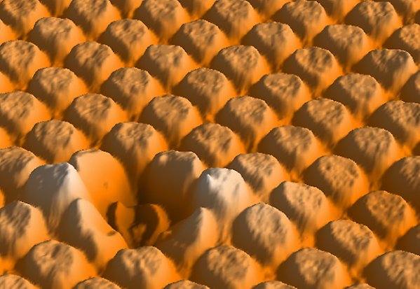
Scanning probe microscopy where a sharp tip is scanned across a surface provides unique information about features on the scale of nanometres.
Atomic force microscopy and scanning tunnelling microscopy can be used to explore surface topography with sub-nanometre resolution. These microscopes are ideal for investigation of patterned materials and nanoparticles. Magnetic force microscopy can be used to image nanoscale magnetic domains.
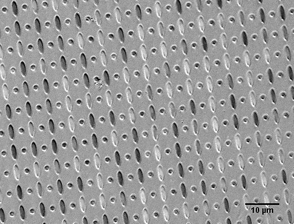
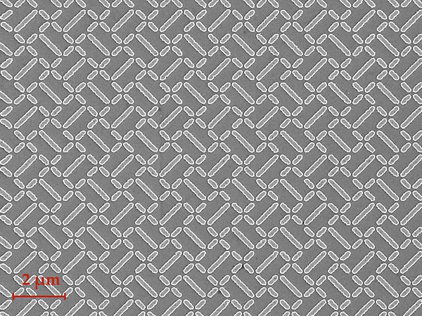
Nanopatterning techniques are used to create artificial 3D islands, allowing us to explore the effects of reduced dimensions and inter-island interactions on material properties.
Electron beam lithography in combination with ion beam milling can produce high-quality arrays of nanostructures over extended areas. Island shapes and sizes as well as the pattern in which they are arranged define their overall properties. As an example we use extended lattices of elongated magnetic islands to study magnetic ordering in frustrated systems known as artificial spin ice. The ordering and dynamics of such systems are explored by magnetic nano-imaging (photoemission electron microscopy).
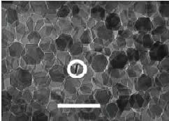
An interesting way to prepare useful nanostructures is to assemble them from atomic or molecular components by careful control of the conditions and interactions of the components so that they naturally self-assemble.
This is the usual approach to building complex structures in nature but is relatively new in nanoscience and nanotechnology. In our group we are interested in both understanding the fundamental aspects of self-assembly and in using these methods to prepare useful sample materials. Current work includes studies of adsorption of polymers and surfactants to interfaces, both as a means to create two-dimensional structures and to modify the interactions of particles so as to control their self-assembly and phase behaviour. A further theme has been to study dispersions of nano-particles or colloids that self-assemble into ordered three-dimensional structures.
Neutron Scattering – SuperADAM and other facilities
This activity is closely related to the Scattering Centre at the Ångström Laboratory (SCÅL) where there is work in most areas of neutron and X-ray scattering. Of special relevance to activities in Materials Physics is the expertise in surface scattering and neutron reflection. Our group shares in the operation and use of the Super ADAM reflectometer at the ILL, Grenoble, France.
Neutron scattering is conventionally used for crystallography (in particular for the location of hydrogen atoms in crystal lattices) and for determination of magnetic ordering and structure. For layered materials, neutron reflectivity gives detailed information on the ordering between magnetic moments in different layers.
A complementary area of expertise is small-angle neutron scattering (SANS). This is widely used to study nanostructures in the bulk. It is particularly exploited in the studies of soft matter.
Another speciality of the group is the study of energetic neutrons in so-called Compton scattering, which is used here for the study of extremely short-lived (10-15 s) quantum correlations between hydrogen atoms in metallic hydrides and other condensed media.
Materials Physics has access to several International neutron facilities such as ILL, ISIS and NIST for these purposes. The group has close links to the Swedish Neutron Scattering Society (SNSS). The society home page provides a range of links to facilities and news in this area. Maths Karlsson is the current chairman of this society. Please contact him for further information.
Contact
- Programme Professor
- Daniel Primetzhofer
- Head of Division
- Gabriella Andersson
- Visiting address: Ångström Laboratory, Lägerhyddsvägen 1, Uppsala, house 4, floor 1 and house 6 floor 1.