Nanoscale patterning and atomic manipulation of 2-dimensional materials
Project and Thesis Topic
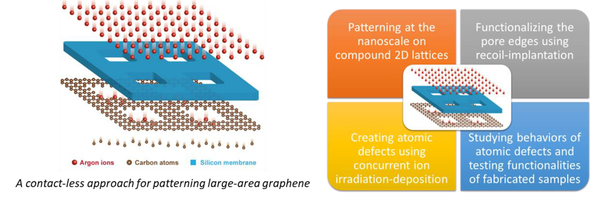
- 2-dimensional (2D) materials have been a research area that leads to many discoveries in recent years. The materials are only one or few atomic layer thick, but have fascinating physical, chemical and mechanical properties [1]. At the same time, there is an immense interest in structuring 2D materials at the nanoscale and at the atomic level for added advanced functionalities. Recently, we have developed a versatile approach capable of structuring the 2D lattices at the nanoscale as well as engineering the materials at the atomic level. The approach relies on a broad and uniform beam of energetic ions passing through a suspended nanopatterned membrane [2].
- The nanopattern membrane, acting as a shadow mask, is fabricated using a multi-step nanofabrication process. Characterization of the structured 2D lattices are done using atomic-resolution transmission electron microscopy (TEM) for studying the atomic defects and the impurities.
Join this project, you will learn:
- Fabricating the nanopattern membranes using nano-microfabrication and ion implantation.
- Characterizing the membrane using electron microscopy (SEM and TEM).
- Fundamental aspects of interactions between energetic ions and 2D materials.
For more information, please email: tuan.tran@physics.uu.se, forskare (research scientist), Department of Physics and Astronomy
References
[1] Geim, A. K. and K. S. Novoselov (2007). "The rise of graphene." Nature Materials 6(3): 183-191
[2 ] Tran, T. T., et al. (2023). "A contactless single-step process for simultaneous nanoscale patterning and cleaning of large-area graphene." 2D Materials 10(2): 025017.
Kontakt
- Programansvarig professor
- Stephan Pomp
- Avdelningsföreståndare
- Henrik Sjöstrand